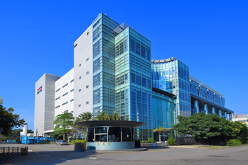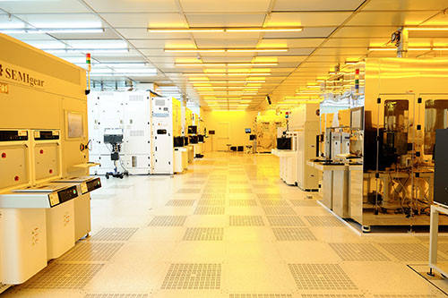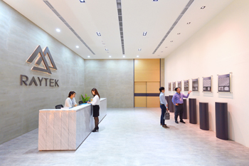
Raytek Semiconductor Inc. (abbreviated as Raytek) was funded in 2016, a high-tech semiconductor company dedicated to wafer-level packages. Raytek was established in Taiwan, and its vision is for the global market, focused on developing wafer-level packages and striving to be the most professional wafer-level RDL/Bumping supplier in Taiwan. Our services include the following:
- Wafer Distribution Layer (CuNiAu RDL & Cu RDL)
- Copper Pillar Bump (CuP Bump)
- Lead-Free Bump (LF Bump)
- Wafer-level Chip Scale Package (WLCSP)
- Application: Cellphones, TVs, printers, monitors, appliances, digit cards, set-top-boxes, bio-chips, and Testing wafers.
- Front Side Metallization (FSM)
- Backside Grinding and Backside Metallization (BGBM)
- Application: Power discreet components such MOSFET and IGBT.
Raytek can provide one-stop and cost-efficient turnkey solutions to customers due to our strategic alliance with professional testing and assembly houses.
Raytek's management and technical team members come from worldwide top-tier assembly houses. The team members could be recognized as the pioneers of Taiwan wafer-level package development, and they deeply understand the history, development trend, and marketing demand in this field. IC design houses worldwide recognize our core team's technological capabilities and operation.
To meet the dynamic challenges in the WLP field, Raytek continues to enhance our core competency with our philosophy of "integrity, pragmatics, innovation, and win-win." We dedicate ourselves to providing excellent products, value-added services, and a working environment that stimulates employee growth. (encourages professional development)
The Raytek Team faces challenges with an open mind, striving for excellence at every opportunity presented. WE WILL NEVER GIVE UP.

2021
Jun.
Joined the Investment Action Plan for Small and Medium Enterprises (SME) supported by the Taiwan Ministry of Economic Affairs
2021
Mar.
Passed the International Automotive Task Force certification (IATF 16949)
2019
Jun.
Launched 8” wafer production line with FSM and BGBM capabilities using Ti, NiV, and Ag.
2018
Jun.
Launched 6” wafer production line for customization on RDL, CuP, LF Bump, Solder Bars, and Dry Film CAP.
2018
Jun.
Passed the certification of IECQ QC080000
2017
Dec.
Passed the certification of ISO 14001 & OHSAS 18001
2017
June.
Passed the certification of ISO 9001
2017
May.
Launched 12” Wafer Production Line For Customization On RDL, CuP, LF Bump.
2017
May.
Low volume production released
2016
Nov.
Clean Room construction complete.
2016
Aug.
First Capital Increase
2016
Apr.


