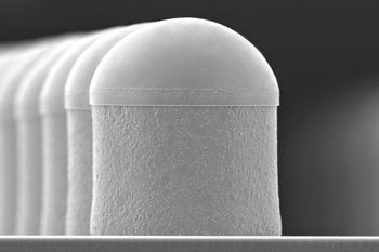
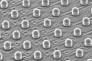
Copper Pillar Bump
Our Copper Pillar Bump improves the packaging capability for flip chips on substrates and modules since it could reach as small as 40um fine bump pitch. Our lead-free solder tip (SnAg1.8%) fulfills RoHS and Green Product requirements. Applications: Dynamic Random Access Memory (DRAM), Memory controller, FPGA, Wi-Fi, RF Switch, Power Control IC, SAW & BAW Filter, and LEDs.
Features
- Wafer Sizes: 12-inch(300mm), 6-inch(150mm)
- Structure & Material: Electroplated solder with SnAg 1.8%, SnAu 80%; Polyimide curing at 200°C (low temp) and 375°C (high temp)
- Bump Pitch: 40μm and above
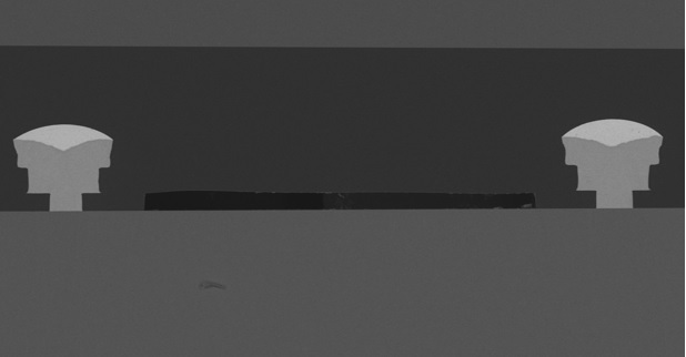
- Pillar Height: 75μm and below for 12-inch wafers; 90μm and below for 6-inch wafers.
- Flexible Design: Asymmetric CPB may provide more design feasibility and enhance electrical and thermal properties.
- Dummy Bump: Provide dummy bump design service to help make flip-chip assembly applicable for chips with only central pads or very few metal pads. The dummy bump and original CPB may stand on different planes while maintaining a level bump surface via flexible bump heights. This service can help facilitate memory devices' flip-chip packaging, such as DRAM.
- Combined Application: Our CPB advantage complements SAW/BAW Filter cavities to protect the sensitive circuit/devices and their products to achieve space efficiency. The optimized features can also greatly enhance the electrical performance and broad application of 5G.
- Turnkey Solution: Provide WLCSP Turnkey Service, including Bumping, Test, Grinding, Dicing, Tape & Reel.
Applications
- Applicable Products: DRAM, Memory controller, FPGA, WiFi, RF Switch, Power Control IC, SAW and BAW Filter, LED...
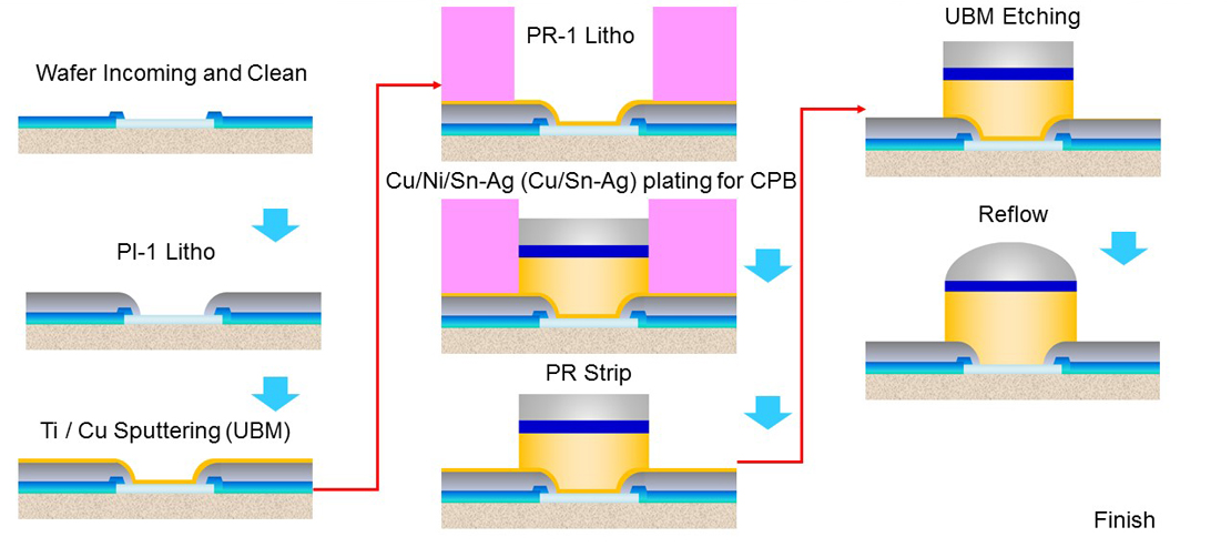
Cu Pillar Bump Process Flow