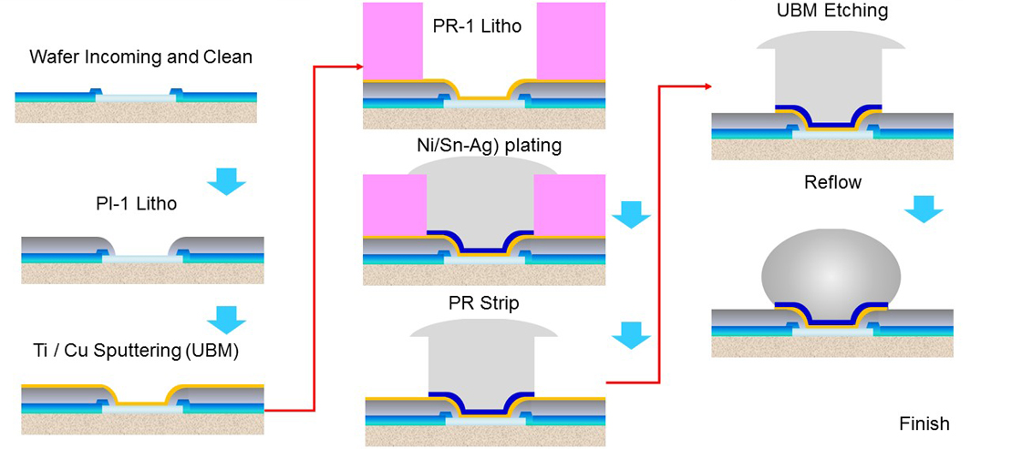
In the family of C4 solder bump, starting from Y1962 IBM high lead (Sn5Pb95) bump then people adopt eutectic bump (Sn63Pb37) for lower working temperature. For environment protection purpose, lead is not allowed to use in electronic industry gradually. LF bump (SnAg1.8) is now the main stream in solder bump and plays as the key process for flip chip with substrate and wafer level CSP on module assembly.
Features
- Support various wafer size: 12-inch(300mm), 6-inch(150mm), 4-inch(100mm)
- Structure & Material: Electroplating solder with SnAg 1.8%, SnAu 80%; Polyimide curing at 200°C(low temp) and 375°C(high temp)
- Bump Pitch: 130 um to 600 um bump pitch with 70 to 250x1800 um UBM size is feasible.
- Bump Height: Bump height can be as high as 100 um.
- Design: Combine with Cu RDL to serve Wafer level CSP application, and Raytek may provide wide UBM size such as 240 um for thin WLCSP package. This is very important for low form factor WLCSP demand for portable devices.
- Turnkey Service: Provide WLCSP Turnkey Service, including Bumping, Test, Grinding, Dicing, Tape & Reel.
Applications
- Applicable Products: DRAM, Nor Flash, Memory controller, FPGA, WiFi, RF Switch, FPGA, Communication Security Chip, Power Control IC, Power Transistor, MEMS, TVS Dipole...


LF Bump Process Flow

