 WHO WE ARE
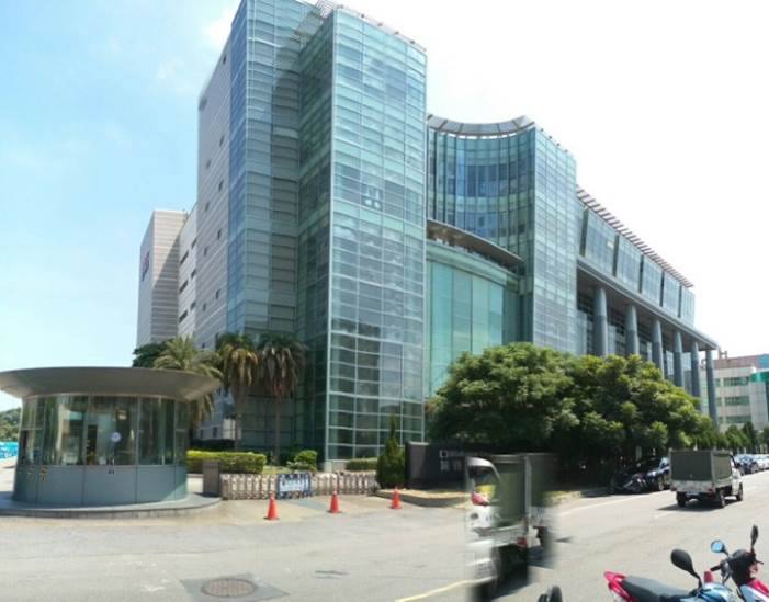
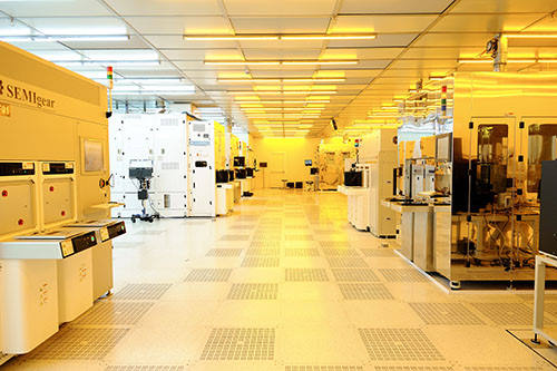
Raytek Semiconductor Inc. (abbreviated as Raytek) was funded on 2016, a semiconductor high tech company dedicated on wafer level package. Raytek is established in Taiwan and its vision is for worldwide market, focused on the development of wafer level package, striving to be the most professional wafer level RDL/Bumping supplier in Taiwan. The product includes CuNiAu RDL, Copper Pillar Bump & Lead Free Bump, which is applied on cell phone, TV, printer, monitoring, appliance, digit card , set-top-box, bio-chip and Testing wafer.. In order to comply with customer’s demand on outsource management, Raytek also has alliance with strategic testing and assembly house to provides one-stop and cost effective service to customers,
The member of Raytek management and technical team all come from worldwide top tier assembly house. The team members could be recognized as the pioneers of Taiwan wafer level package development, they deeply understand the history, development trend and marketing demand in this field. Our core team’s capability of technology and operation is well recognized by IC design house.
To meet the dynamic challenge in this package field, Raytek continues to enhance our core competence, with our philosophy of “integrity, pragmatics, innovation, win-win”, dedicate ourselves to provide satisfactory product and value-added service, also to provide the working environment for every employee to grow.
Raytek employee are all with attitude of open-mind, striving for excellence, facing challenge, optimistic and we will never give up.
 Company Roadmap
2017
June.
Pass the certification of ISO 9001
2017
May.
Low volume production released
2016
Apr.
Raytek Funded with capital NTD $29M
2016
Aug.
Fund-rising to NTD $913M
2016
Nov.