Lead Free Bump (LFB)
In the family of C4 solder bump, starting from Y1962 IBM high lead (Sn5Pb95) bump then people adopt eutectic bump (Sn63Pb37) for lower working temperature. For environment protection purpose, lead is not allowed to use in electronic industry gradually. LF bump (SnAg1.8)is now the main stream in solder bump and plays as the key process for flip chip with substrate and wafer level CSP on module assembly.
Raytek offers
- 130 um to 200 um bump pitch with 70 to 100 um UBM size is feasible
- Bump height can be as high as 100 um
- Polyimide curing at 200 degree C prevents Memory device suffering data retention rate
- Polyimide curing at 375 degree C for logic device is served
- Combine with Cu RDL to serve Wafer level CSP application
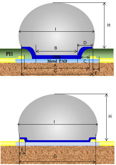
| Label | Description | Design Rule(um) |
|---|---|---|
| A | Mini PSV opening | ≥ 40 |
| B | Mini PI opening (HD4104) | ≥ 20 |
| Mini PI opening (BM300) | ≥ 30 | |
| C | PSV enclosure by PI | ≥ 5 |
| D | PI enclosure by UBM | ≥ 15 |
| E | UBM enclosure by metal pad | ≥ 2 |
| F | PSV opening enclosure by UBM | ≥ 10 |
| Label | Description | Bump pitch (um) | |||||||
|---|---|---|---|---|---|---|---|---|---|
| 130~150 | 150~175 | 175~200 | 200~225 | ||||||
| G | UBM width | 70 | 80 | 80 | 80 | 88 | 88 | 100 | 108 |
| H | Bump height | 70 | 80 | 80 | 80 | 90 | 90 | 90-100 | 90-100 |
| I | Bump height | 90 | 100 | 100 | 100 | 110 | 110 | 123-130 | 126-133 |
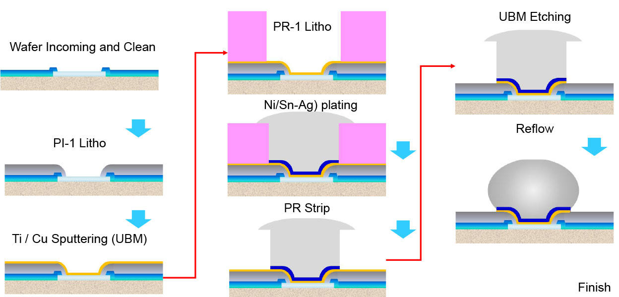
LF Bump Process Flow