Copper Pillar Bump
Copper Pillar Bump improves the package capability for flip chip on substrate and flip chip on module since it could reach as small as 50 um fine bump pitch. The lead free solder tip (SnAg1.8%) can meet RoHS and Green Product requirement.
Raytek offers
- 40 um pitch with 25 um bump size CPB is available, up to 150 um bump pitch is feasible
- Bump height can as high as 75 um, 135 um is available for sample
- Polyimide curing at 200 degree C prevents Memory device suffering data retention rate
- Polyimide curing at 375 degree C for logic device is served
- Both Cu/SnAg and Cu/Ni/SnAg CPB are feasible for bump structure
- PI pull-in and pull-out with Al pad exposure design is available for design flexibility
| Products | Cu Pillar | Cu Pillar Bump | Lead Free Bump | Cu RDL + LFB |
|---|---|---|---|---|
| PI | 5 um | 5 um | 5 um | 5 um |
| PVD1 Ti/Cu | 0.1/0.2 um | 0.1/0.2 um | 0.1/0.5 um | RDL 0.1/0.2 um UBM 0.1/0.5 um |
| ECD Cu | 65 ~ 2 um | 35 ~ 7 um | - | 3 um RDL |
| ECD Ni | - | 3 um | 3 um | 3 um |
| ECD SnAg(1.8%) | - | 35 ~15 um | ≦100 um | ≦100 um |
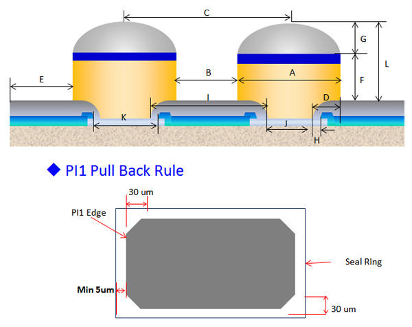
| Symbol | Description | Design Rule |
|---|---|---|
| A | Bump size (PI1:HD4104) | Min. 35 um |
| Bump size (PI1:BM300) | Min. 45 um | |
| B | Bump space | Min. 15 um |
| C | Bump pitch (PI1:HD4104) | Min. 50 um |
| Bump pitch (PI1:BM300) | Min. 60 um | |
| D | Bump edge to PI1 opening | Min. 7.5um |
| E | Bump edge to die edge | Min. 50 um |
| F | Cu post height | ≦ Bump Size |
| G | Solder cap height | ≦1/2 Bump Size |
| H | PI1 to PSV overlap | Min. 5 um |
| I | PI1 width | Min. 35 um |
| J | PI1 opening (PI1:HD4104) | Min. 20 um |
| PI1 opening (PI1:BM300) | Min. 30 um | |
| K | PSV opening (PI1:HD4104) | Min. 30 um |
| PSV opening (PI1:BM300) | Min. 40 um | |
| L | Bump height (before reflow) | Max. 60 um |
| Bump height (after reflow) | Max. 75 um | |
| Fuse exposure | Not allow | |
| Bump plating ratio | 1.47~88.38 % (Machine Limit) |
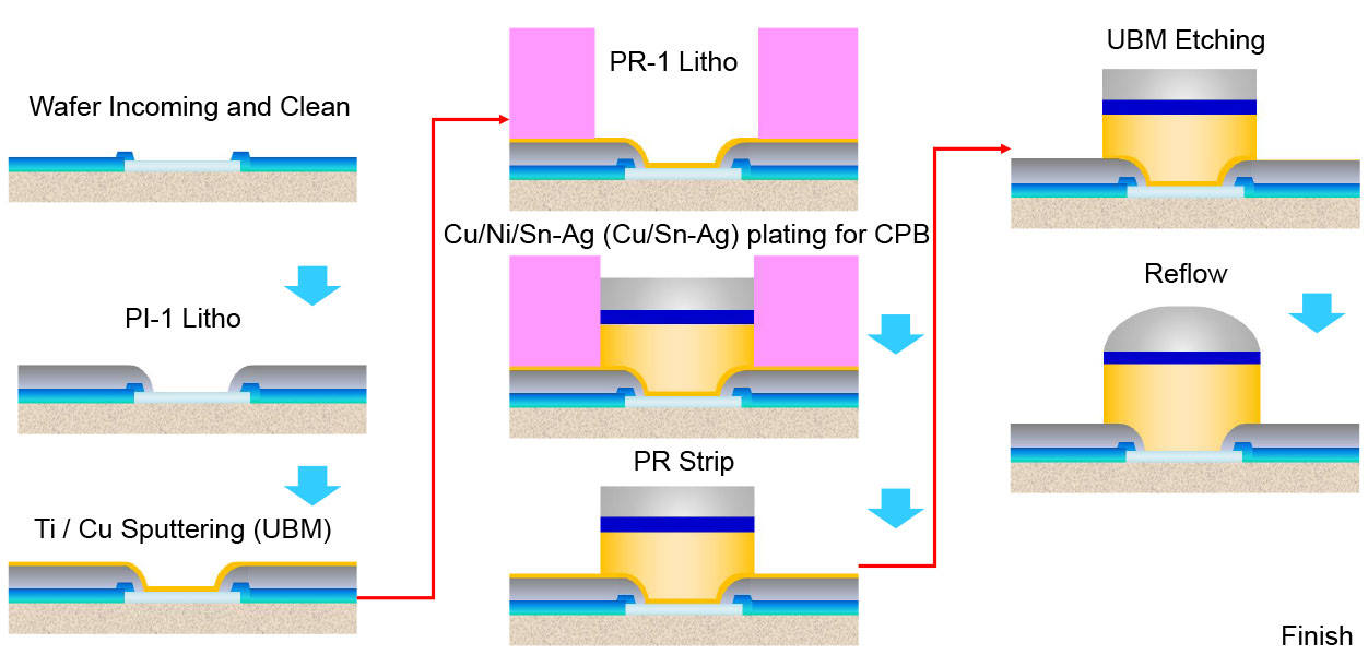
Cu pillar Bump Process Flow