WAFER LEVEL CHIP SCALE PACKAGE
Definition of WLCSP is Package IC, compatible with standard PCB interconnect technology and with a size equal to the chip size, fabricated using wafer-level process. Currently, only plating technology is applied. Applications: DRAM, Nor Flash, FPGA, Communication Security Chip, Power Transistors.
Features
- Wafer Size: 12-inch(300mm), 6-inch(150mm)
- Structure & Material: Electroplating solder with SnAg 1.8%, SnAu 80%; Polyimide curing at 200°C (low temp) and 375°C (high temp)
- Bump Height: Standard bump height is between 68um and 167um, adjusted according to customer requirements.
- Design: Combined with Cu RDL to serve Wafer-level CSP applications, Raytek may provide wide UBM sizes such as 240um for thin WLCSP packages. This is very important for low form factor WLCSP demand for portable devices..
- Turnkey Service: Provide WLCSP Turnkey Service, including Bumping, Test, Grinding, Dicing, Tape & Reel.
Applications
- Applicable Products: DRAM, Nor Flash, FPGA, Communication Security Chip, Power Transistor, ...
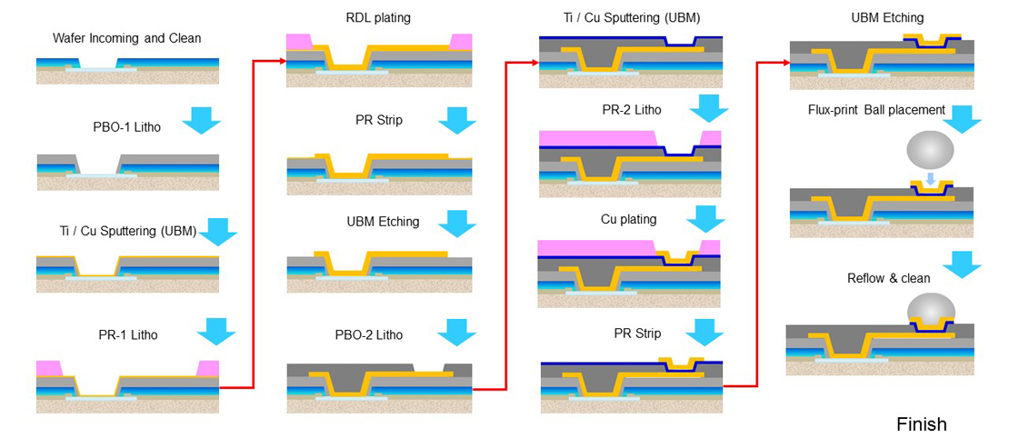
WLCSP Process Flow- Plating
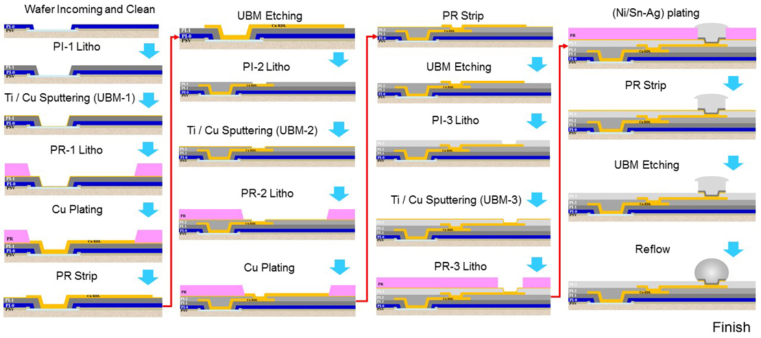
WLCSP Process Flow- Ball Placement