WAFER DISTRIBUTION LAYER
Small form factor, lower power consumption, and high-performance product with low cost create strong market demand for RDL in memory, which can re-route I/O and make integration of MCP (Multi-Chip-Package) and SiP (System in Package) achievable. Application: DRAM, Nor Flash, Wi-Fi, RF Switch, FPGA, Communication Security Chip, and Power Transistor.
Features
- Wafer Size: 12-inch(300mm), 6-inch(150mm)
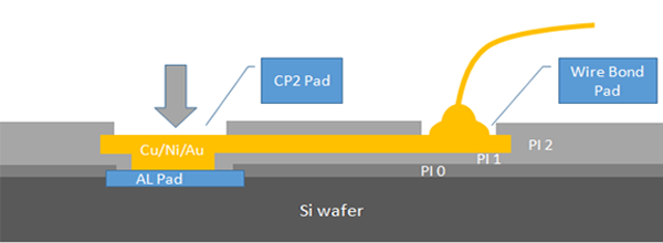
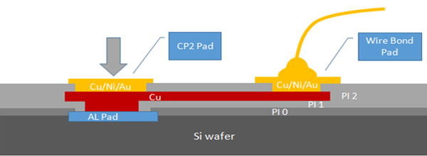
- Structure & Material: Cu/Ni/Au RDL to support Memory makers in flexible pad layout KGD to meet variant end-users in SiP design. This KGD chip is compatible with Au and Cu wire bonds in the assembly process. Polyimide curing at 200°C (low temp) and 375°C (high temp).
- Design: Cu RDL combines with copper pillar bump or lead-free bump to serve Fan-in & Fan-out WLCSP.
- Base Material: RDL on glass serves to advance package with glass carrier.
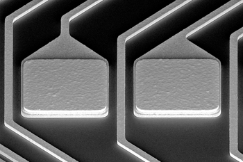
- Trace Width: 5/5 um fine pitch RDL is suitable for design feasibility, and it has the same wire bond compatibility with Au wire and Cu wire bond as the standard RDL (Ultra Slim RDL).
- Turnkey Solution: Provide WLCSP Turnkey Service, including Bumping, Test, Grinding, Dicing, Tape & Reel.
Applications
- Applicable Products: DRAM, Nor Flash, WiFi, RF Switch, FPGA, Communication Security Chip, Power Transistor, ...
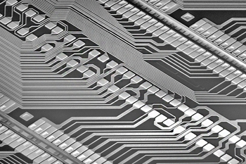
1RDL Fine Line solution (5/5)
8 um/8 um STD RDL
5 um/5 um Fine Pitch
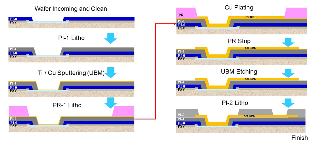
Process Flow of RDL (2P1M)